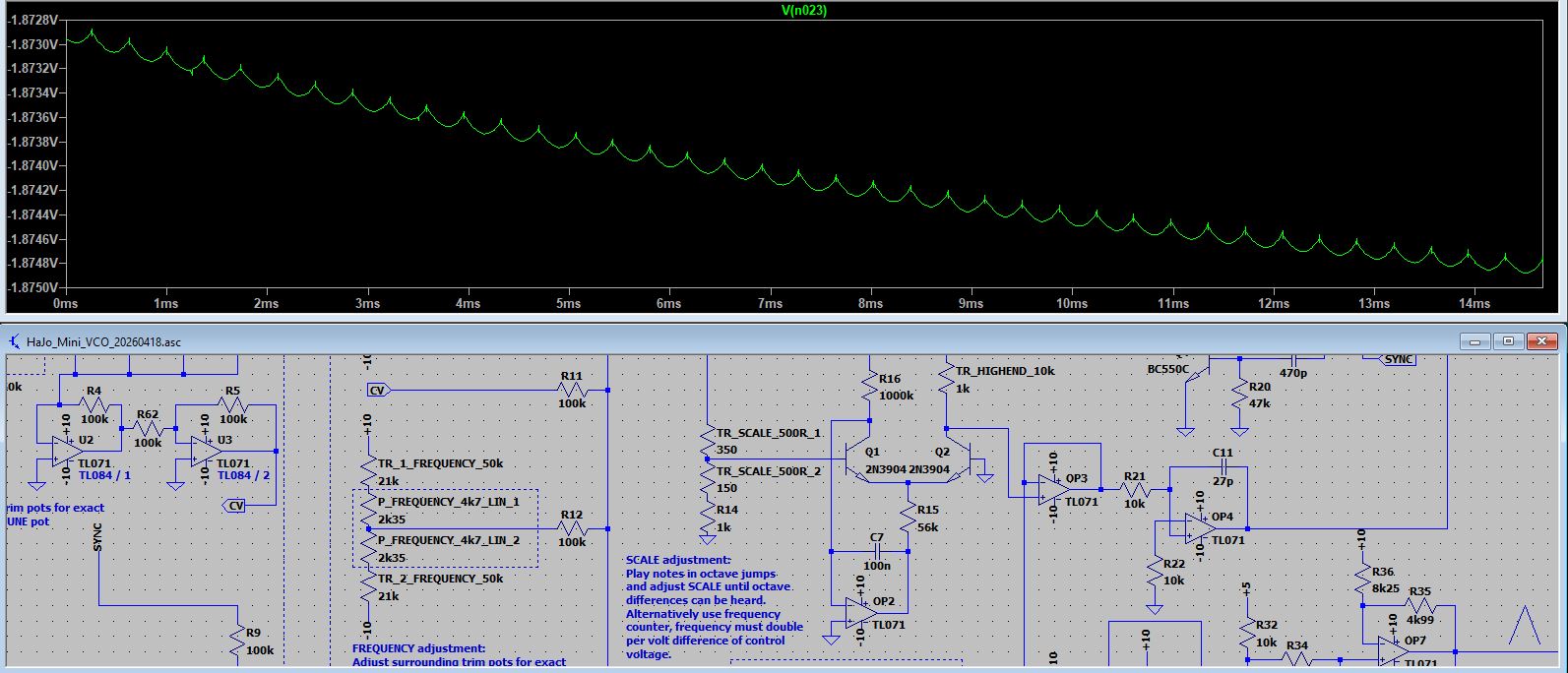
The situation is following:The diagram shows part of the schematic for the late-model Minimoog VCO-102. In the circuit, Q7 and Q8 form a current sink, drawing a current through the collector of Q7 that is exponentially related to the voltage present at the base of Q7. This current is integrated by C7 until the voltage at the drain of Q4 (which is at present switched off) reaches 0V as detected via the voltage follower IC7 by the comparator IC8b, whose + input is held close to ground by a resistor not shown. At this point, the capacitor is discharged by Q4, and the drain of Q4 rises to 5V again. Thus the oscillator generates a falling sawtooth waveform with a frequency proportional to the current. Compensating resistor R31 can be neglected at low frequencies, and the purpose of Q5 is just to lift the sawtooth at the base of Q6 (which converts the sawtooth to a triangle wave) by 1 V_BE drop. IC8b has a bit of positive feedback to ensure a clean reset.
Further analysis is given in the Minimoog Service Manual, Section 2.3, which can be found online: http://www.cyborgstudio.com/synthmp3s/moog/minimoog/manual/minimoogservicemanual.pdf
Note that
(a) The collector of Q8 is held at ground by the negative feedback around op-amp IC6.
(b) So 5 microamps flow in R30 as claimed on the schematic [though in the opposite direction to that marked].
(c) The emitters of Q7 and Q8 are held at a V_BE drop (appropriate to I_C = 5 μA) below ground by action of the op-amp.
(d) When the base of Q7 is at ground potential, 5 μA will flow in Q7 also.
(e) This will charge C7 to 5V in 1ms, and give the oscillator a frequency of 1kHz, assuming reset time is negligible. Indeed the legend 200Hz/μA appears above R30.
(f) But the legend 0.00mV = 2’ lo F = 350Hz appears at the base of Q7, implying that setting the oscillator’s range switch to the highest (2 foot) setting and pressing the bottom note on the keyboard will produce a voltage of 0.00 mV here and a frequency of 350Hz. And indeed, taking A4 = 440Hz gives F4 = 349.23Hz according to [an online source].
These things can’t all be true at once! Is it just (f) that’s wrong, or is there some reason why the current sink doesn’t give 5 μA but something more like 5/3 μA when Q7’s base is at ground?
Bonus question: what is the purpose of CR2 in this circuit?
Thanks.