A couple more questions, if I may....
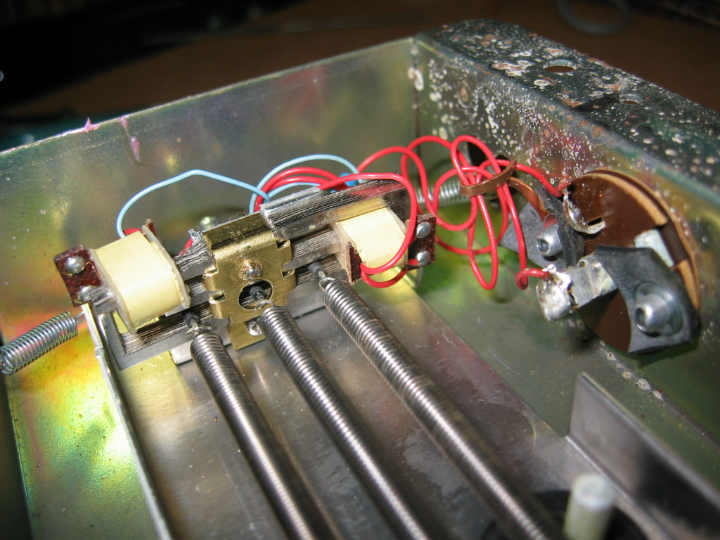
1) At the bottom left quadrant, there's a 10uf blue cap, a 220 ohm resistor, then a resistor that I think is a 33k, but is hidden from view by the big brown .22uf cap next to it.
Could you move that cap over to the right a bit and get a shot of whatever is stuffed there?
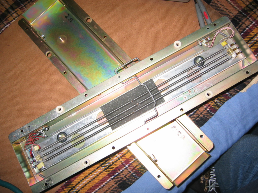
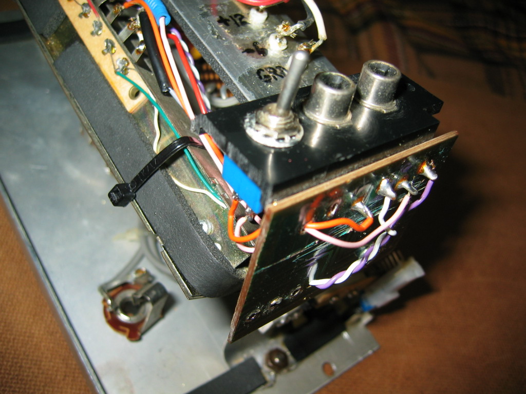
2) Also, below that 100k resistor a bit to the right is a bunch of wires connecting out to the various jacks and pot connections. Buried under that bundle of wires, I believe that there is a bare wire jumper installed on top that connects two close by pads (below the 100k, and to the right of the 15k).
I think I can see it a bit in your current picture, but could you verify that its really there?
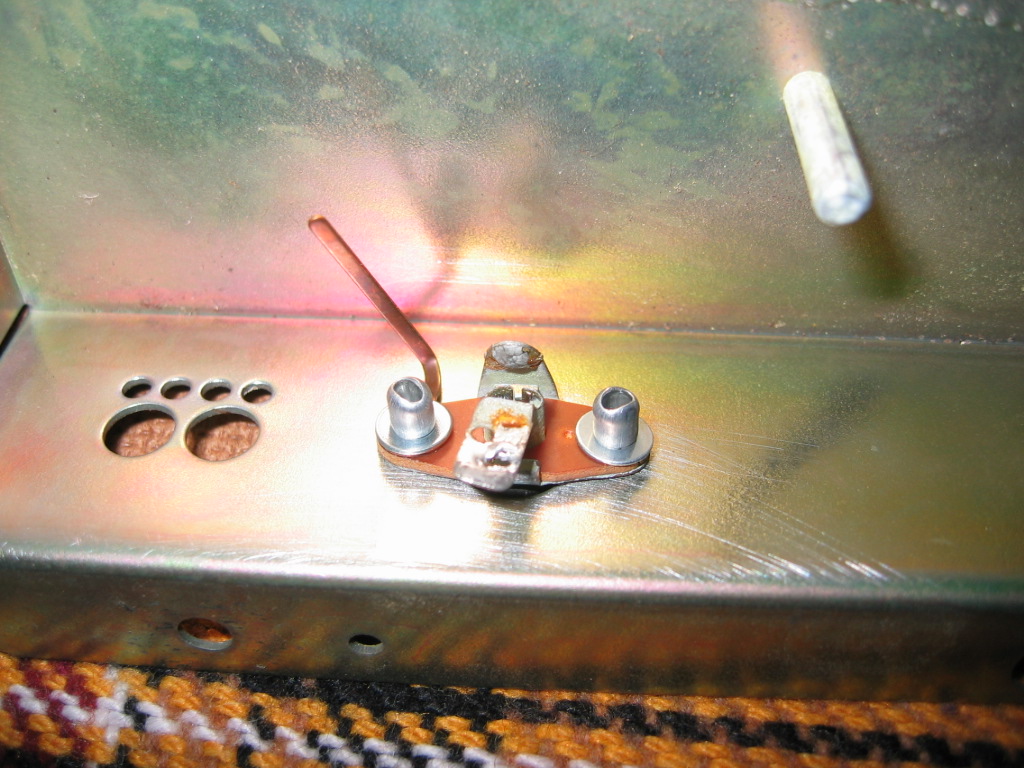
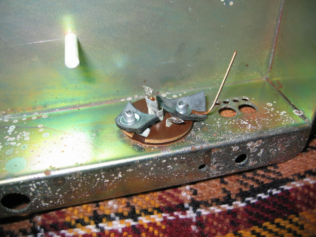
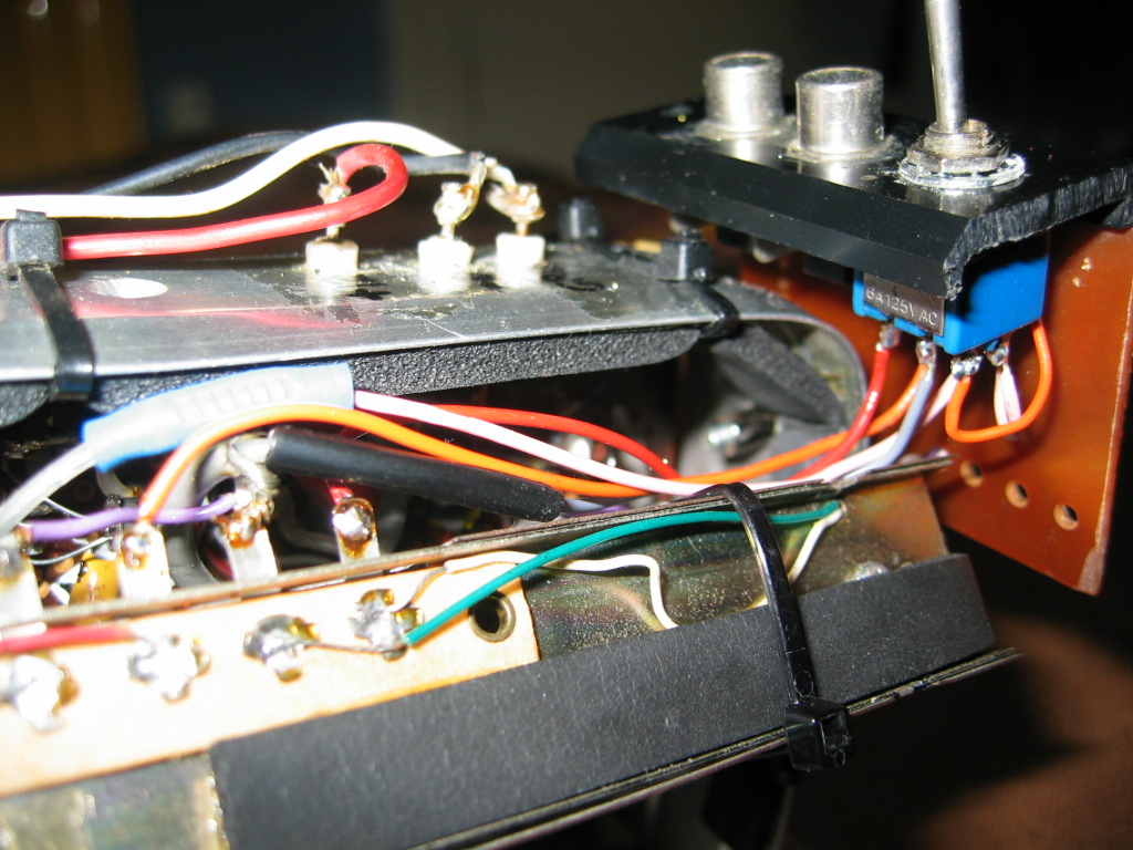
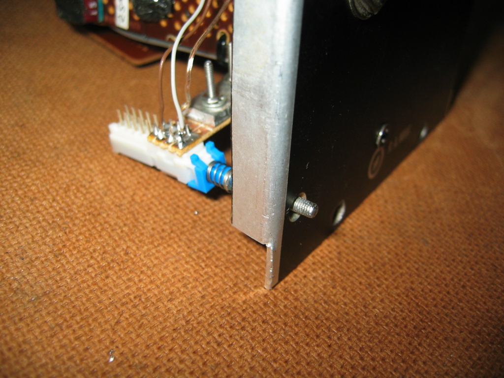
3) If you have an ohmmeter, could you ohm between that upper trace that the screw and big solder lug are connected to, and see if it is connected to pin2, or to pin 3 on the power connector.
I believe that this is connected to pin 3 (-6v). Lots of reverb springs have the return jack grounded to the metal chassis of the unit for shielding, while the input jacks are completely floating.
However, in your pictures, there appears to be nothing connected to the pin 3 trace, at least not on the top where we can see. There may be something soldered on the back (trace) side which I can't see.
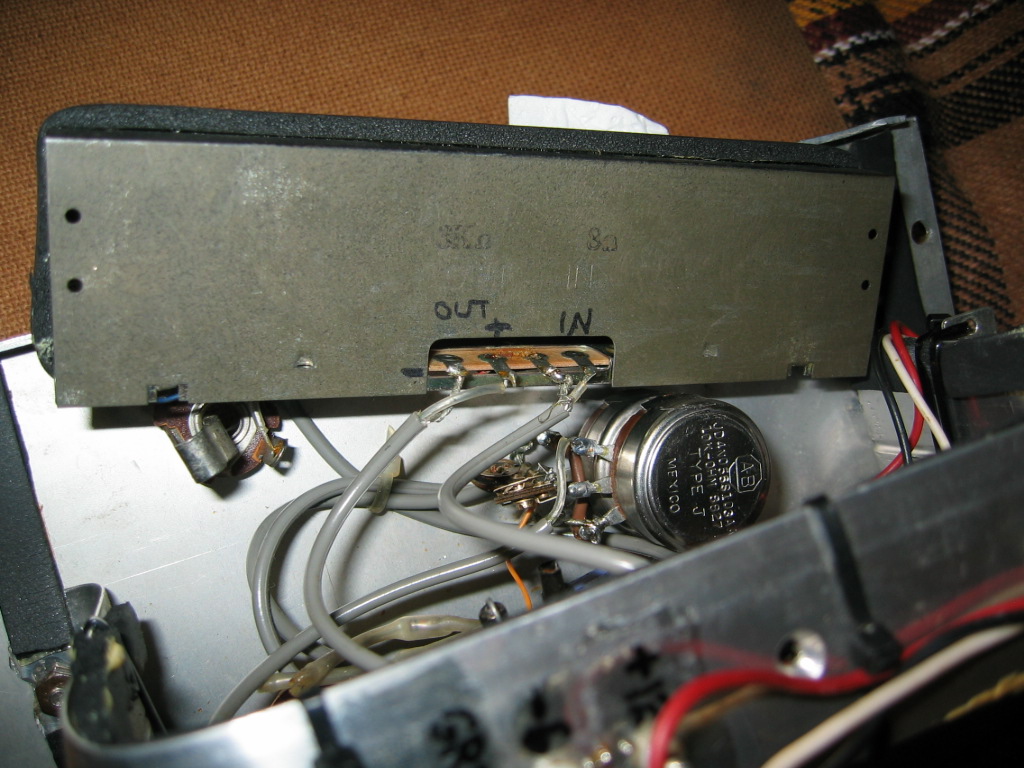
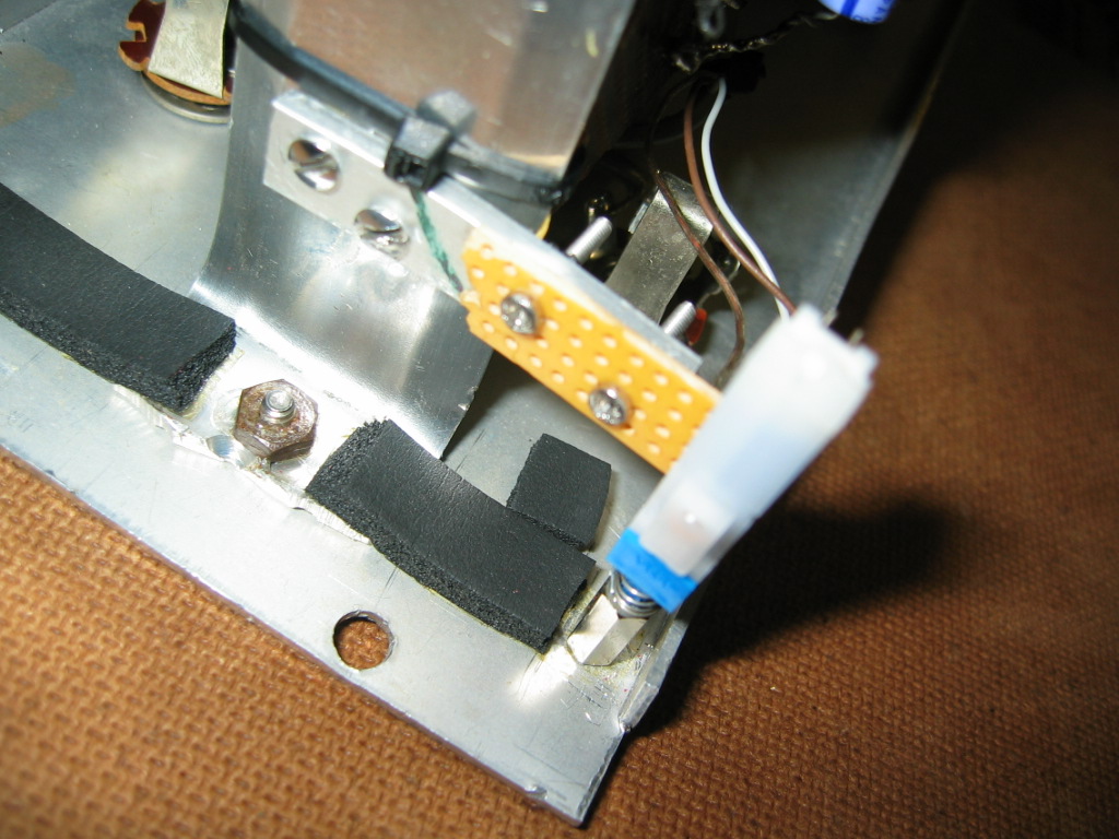
There appears to be two wires (a green and a black one) soldered to the chassis of the reverb springs near the RCA output jack. Where do these go?
My thoughts are that there's a wire connected from pin 3 to the hole that the solder lug is soldered to, and in turn to the chassis of the reverb springs. This would supply the -6v to the reverb return "ground" shown in the schematics. There's also the chance that the green wire is the one we see coming down the connector side to connect to what I think is the ground trace at the top of the 100k. Perhaps the -6V is not used at all?
Is any of this close?
The 2N3391 makes sense, as Moog used lots of these in later builds, and from what I saw of the way the transistor pads are laid out, they all have the same pinout. If the transistor shown in the schematic for Q1 were used, it would have to have the leads rearranged to properly work with this layout.
Thanks again for your help!

![[url=https://flic.kr/p/E6nKMZ][img]http ... .jpg[/img]](%5Burl=https%3A//flic.kr/p/E6nKMZ%5D%5Bimg%5Dhttps://farm2.staticflickr.com/1708/25002384335_ae0b003046_o.jpg%5B/img%5D)
![[url=https://flic.kr/p/DDgi2s][img]http ... .jpg[/img]](%5Burl=https%3A//flic.kr/p/DDgi2s%5D%5Bimg%5Dhttps://farm2.staticflickr.com/1599/24706894720_3f8c484b17_o.jpg%5B/img%5D)
![[url=https://flic.kr/p/D8DKeN][img]http ... .jpg[/img]](%5Burl=https%3A//flic.kr/p/D8DKeN%5D%5Bimg%5Dhttps://farm2.staticflickr.com/1589/24371780484_20d4228ae9_o.jpg%5B/img%5D)
![[url=https://flic.kr/p/D8Z5TD][img]http ... .jpg[/img]](%5Burl=https%3A//flic.kr/p/D8Z5TD%5D%5Bimg%5Dhttps://farm2.staticflickr.com/1700/24375553723_31439b25f3_o.jpg%5B/img%5D)
![[url=https://flic.kr/p/DUWVj1][img]http ... .jpg[/img]](%5Burl=https%3A//flic.kr/p/DUWVj1%5D%5Bimg%5Dhttps://farm2.staticflickr.com/1719/24884373592_a359bbff7c_o.jpg%5B/img%5D)
![[url=https://flic.kr/p/DDgh33][img]http ... .jpg[/img]](%5Burl=https%3A//flic.kr/p/DDgh33%5D%5Bimg%5Dhttps://farm2.staticflickr.com/1591/24706891390_eeab94ac49_o.jpg%5B/img%5D)
![[url=https://flic.kr/p/DUWUDy][img]http ... .jpg[/img]](%5Burl=https%3A//flic.kr/p/DUWUDy%5D%5Bimg%5Dhttps://farm2.staticflickr.com/1469/24884371362_0fdbff2dfb_o.jpg%5B/img%5D)
![[url=https://flic.kr/p/DwTza8][img]http ... .jpg[/img]](%5Burl=https%3A//flic.kr/p/DwTza8%5D%5Bimg%5Dhttps://farm2.staticflickr.com/1466/24634757549_ac99f24e76_o.jpg%5B/img%5D)
![[url=https://flic.kr/p/E6nHyF][img]http ... .jpg[/img]](%5Burl=https%3A//flic.kr/p/E6nHyF%5D%5Bimg%5Dhttps://farm2.staticflickr.com/1634/25002376835_ee754eb64e_o.jpg%5B/img%5D)
![[url=https://flic.kr/p/DX8B7V][img]http ... .jpg[/img]](%5Burl=https%3A//flic.kr/p/DX8B7V%5D%5Bimg%5Dhttps://farm2.staticflickr.com/1561/24909091621_51a3c5e707_o.jpg%5B/img%5D)
![[url=https://flic.kr/p/D8Z3Ea][img]http ... .jpg[/img]](%5Burl=https%3A//flic.kr/p/D8Z3Ea%5D%5Bimg%5Dhttps://farm2.staticflickr.com/1545/24375546213_dac5d20bbc_o.jpg%5B/img%5D)